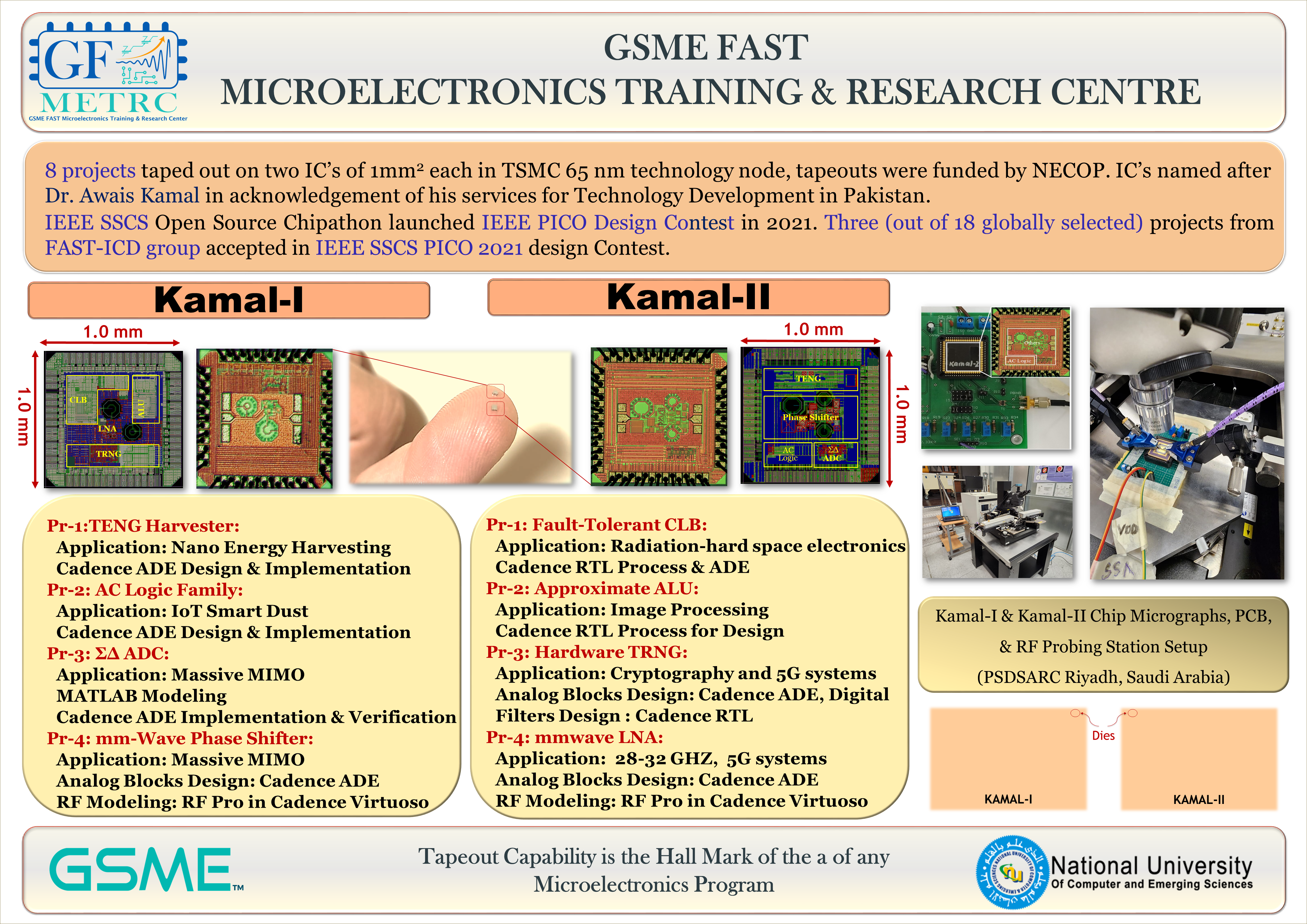
Graduate Student Projects
PICO Tapeout: 3 Projects
SUb-6 GHz Bidirectional Amplifier:
- Application: sub-6 GHz RF front ends
- Tools: Xschem, Ngspice, Magic, Netgen
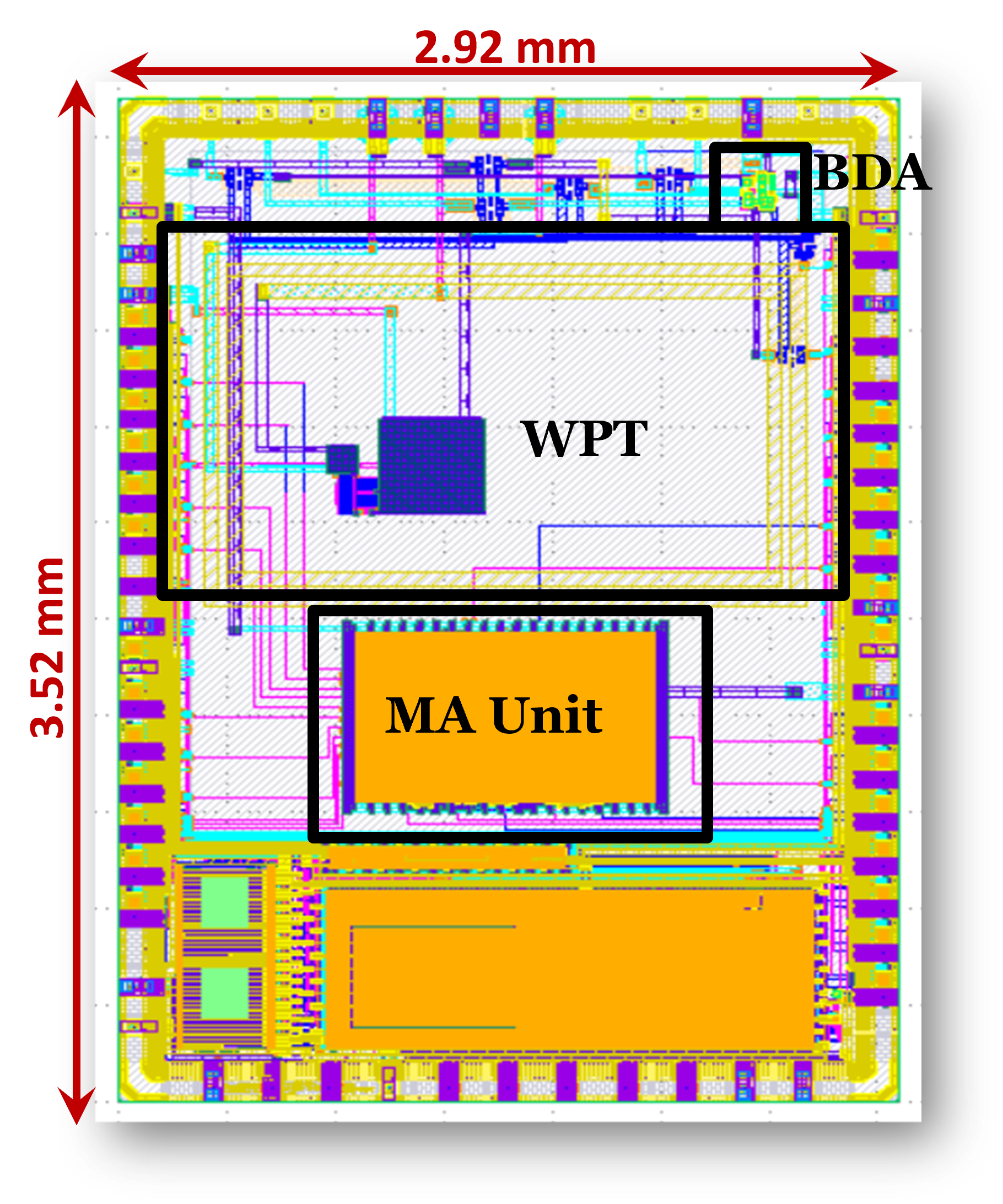
Backscattering Integration in WPT:
- Application: Wireless Power Transfer
- Tools: Xschem, Ngspice, Magic, Netgen, ADS(For Inductor Modelling)
64-bit MA Unit:
- Application: ALUs
- Tools: RTL Vivado, Cadence, Genus, Innovus
Tapeout: 05 November, 2021
Kamal 1 Projects
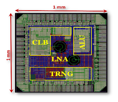
Fault-Tolerant CLB:
- Application: Radiation-hard space electronics
- Cadence RTL Process
Approximate ALU:
- Application: Image Processing
- Cadence RTL Process for Design
Hardware TRNG:
- Application: Cryptography and 5G systems
- Analog Blocks Design: Cadence ADE, Digital Filters
- Design: Cadence RTL
mm-Wave Phase Shifter:
- Application: 5G Systems
- 28-32 GHZ
- Analog Blocks Design: Cadence ADE
- RF Modeling: RF Pro in Cadence Virtuoso
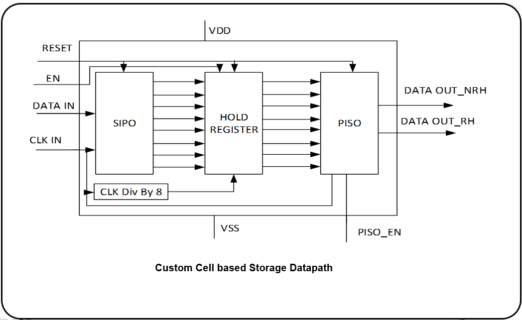
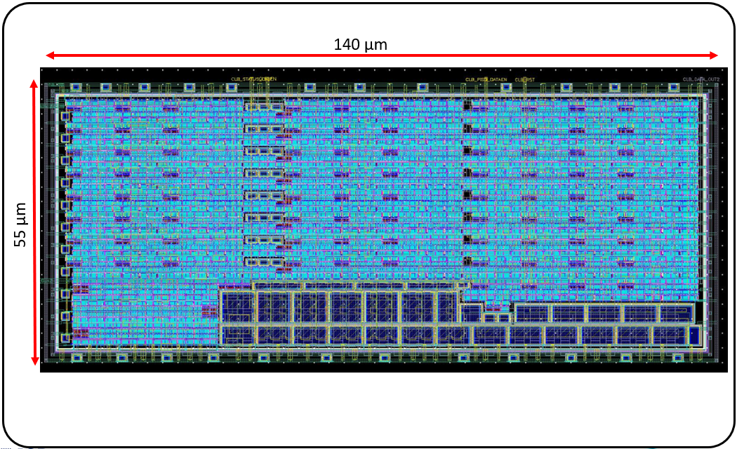
FAULT TOLERANT CLB FOR HIGH RELIABILITY AUTONOMOUS APPLICATION
Block Diagram
Layout
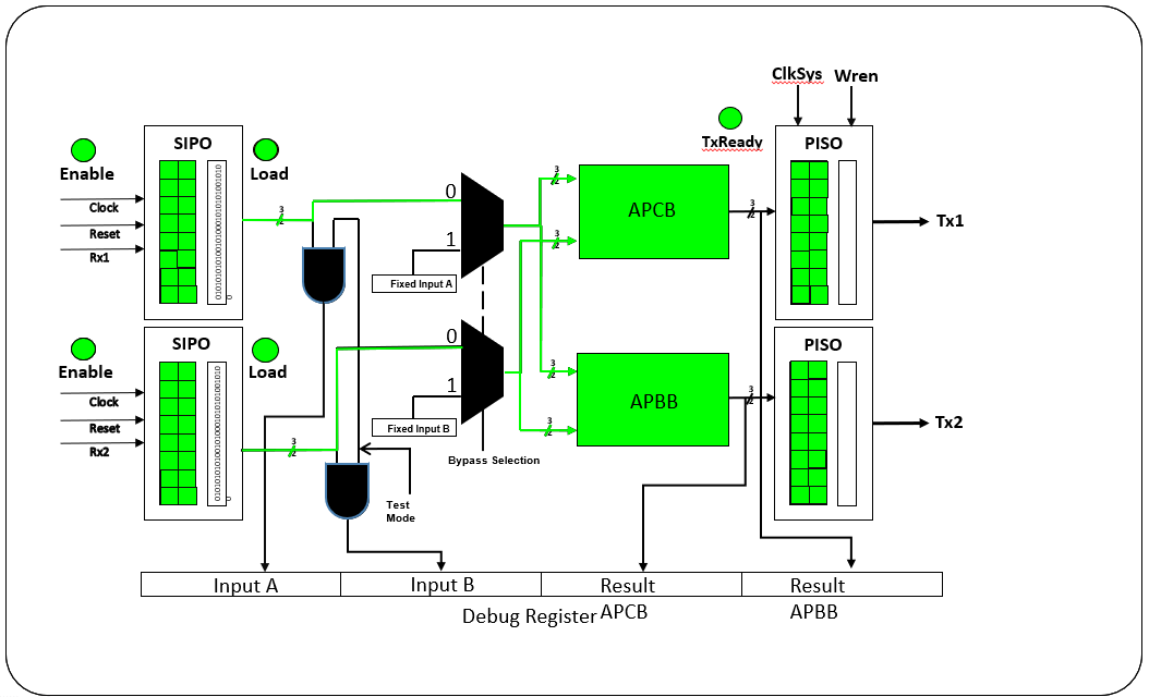
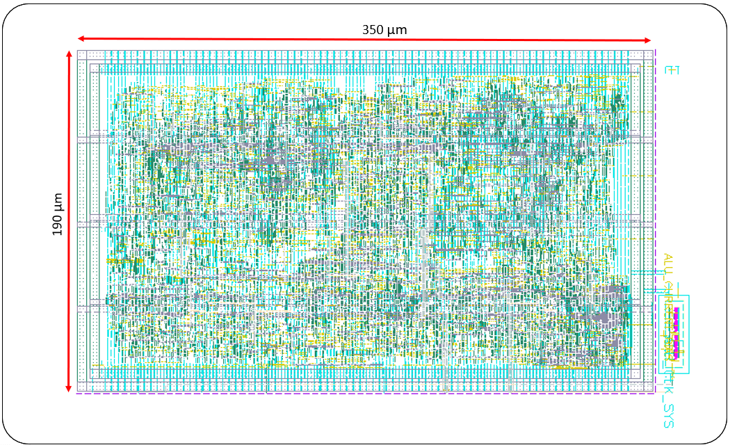
ASIC Implementation of ALU Based on Approximate Computing
Block Diagram
Layout
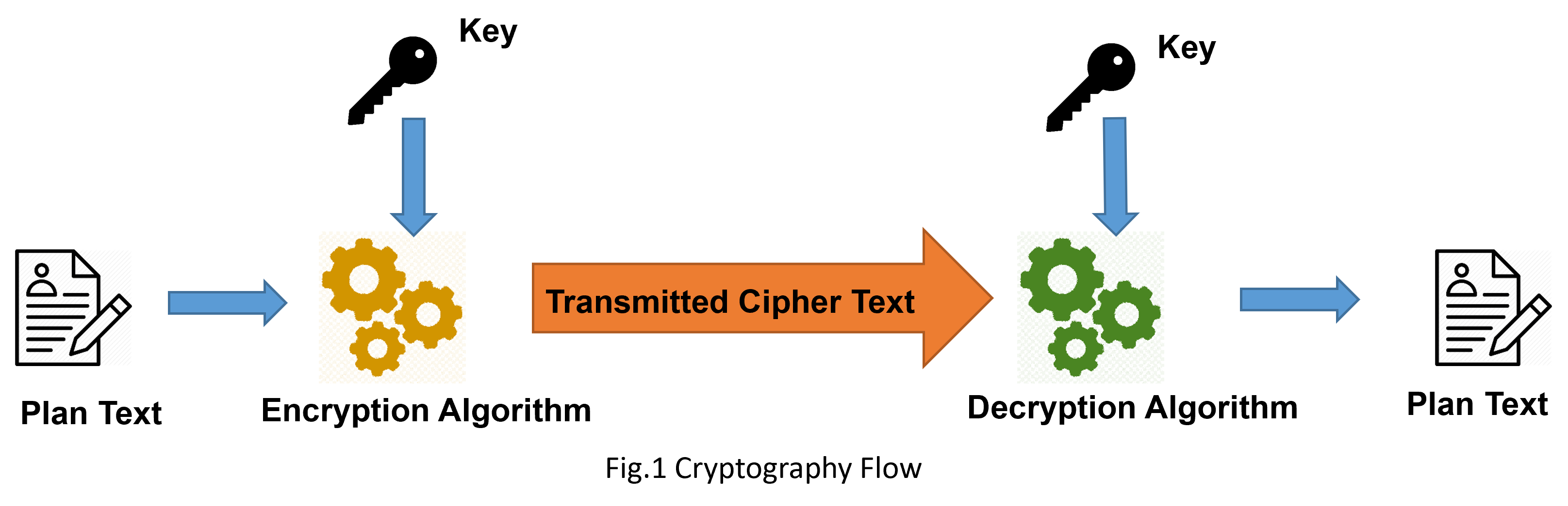
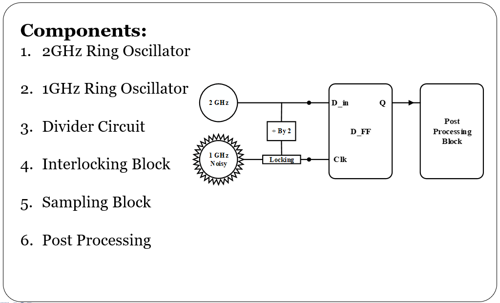
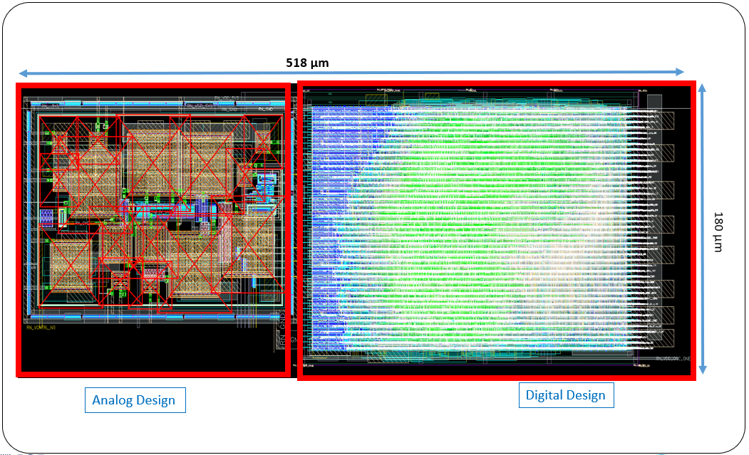
Hardware True Random Number Generator
Cryptography Requirements
- Conditionally Secure
- Computationally Secure
Block Diagram
Layout
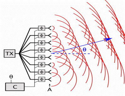
mm-Wave LNA for MMIMO Applications
Motivation
- Modern 5G (and beyond) Communication technology will be based on Massive MIMO architectures
- MMIMO architectures make extensive use of beamforming
- Beamforming and MIMO require multiple transmitter and receiver chains
- RF front end of each transceiver chain consists of a microwave circuits
- Crucial component is the Low Noise Amplifier (LNA) in the receiver chain
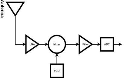
Block Diagram
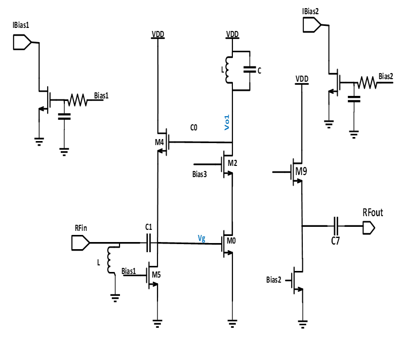
Layout
Kamal 2 Projects
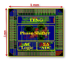
TENG Harvester:
Application: Nano Energy Harvesting
Cadence ADE Design & Implementation
AAC Logic Family:
Application: IoT Smart Dust
Cadence ADE Design & Implementation
ΣΔ ADC:
Application: Massive MIMO
MATLAB Modeling
Cadence ADE Implementation & Verification
mm-Wave Phase Shifter:
Application: Massive MIMO
Analog Blocks Design: Cadence ADE
RF Modeling: RF Pro in Cadence Virtuoso
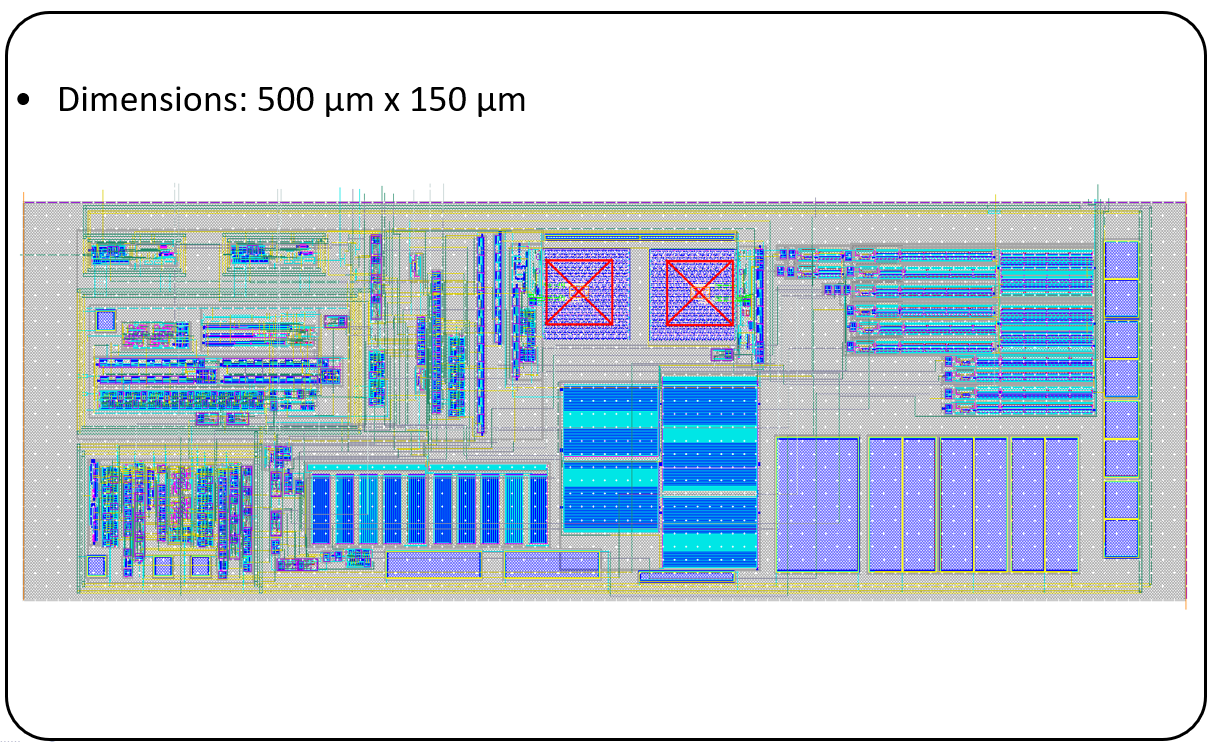
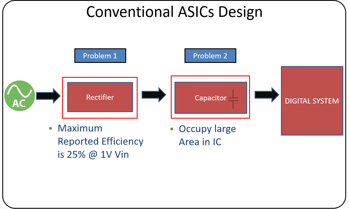
Capacitor-less High Efficiency Triboelectric Energy Harvester with Voltage Biasing
Block Diagram
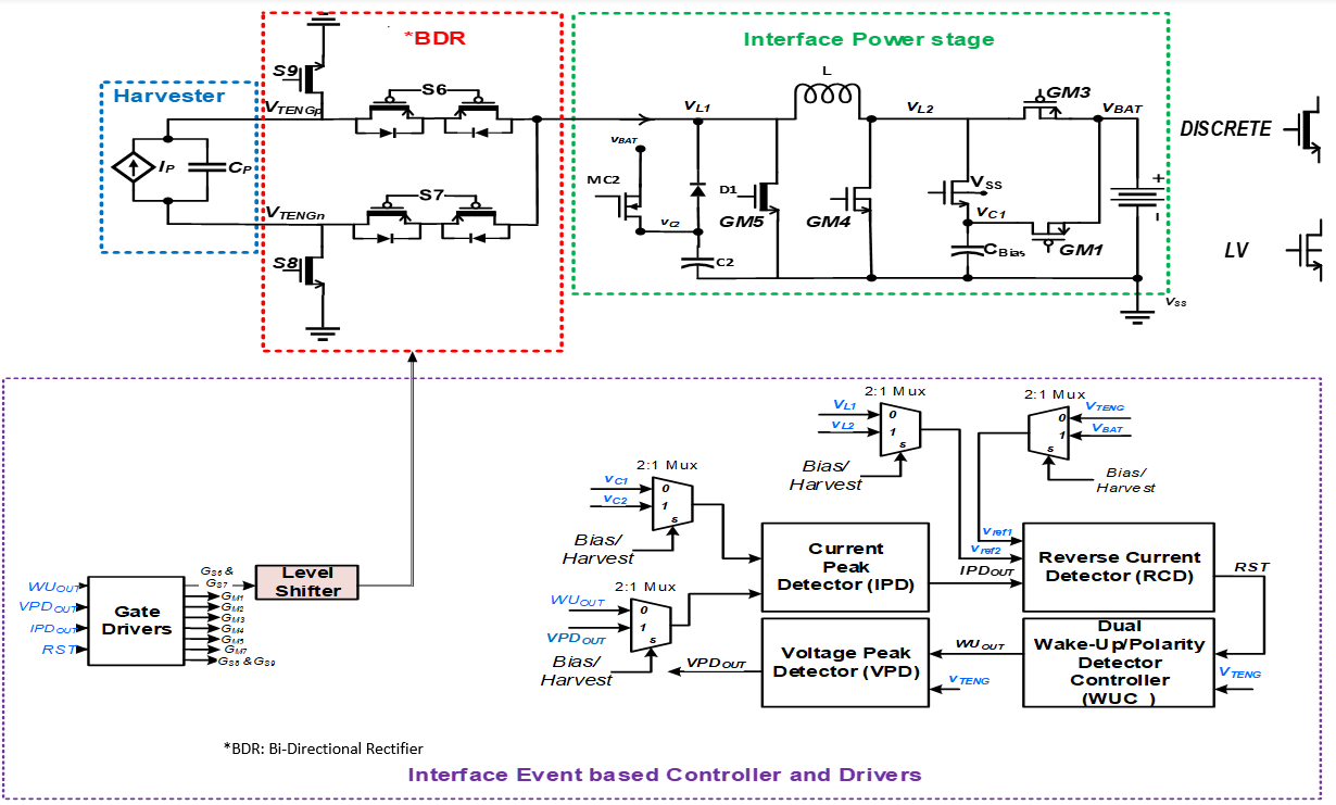
Layout
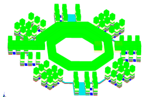
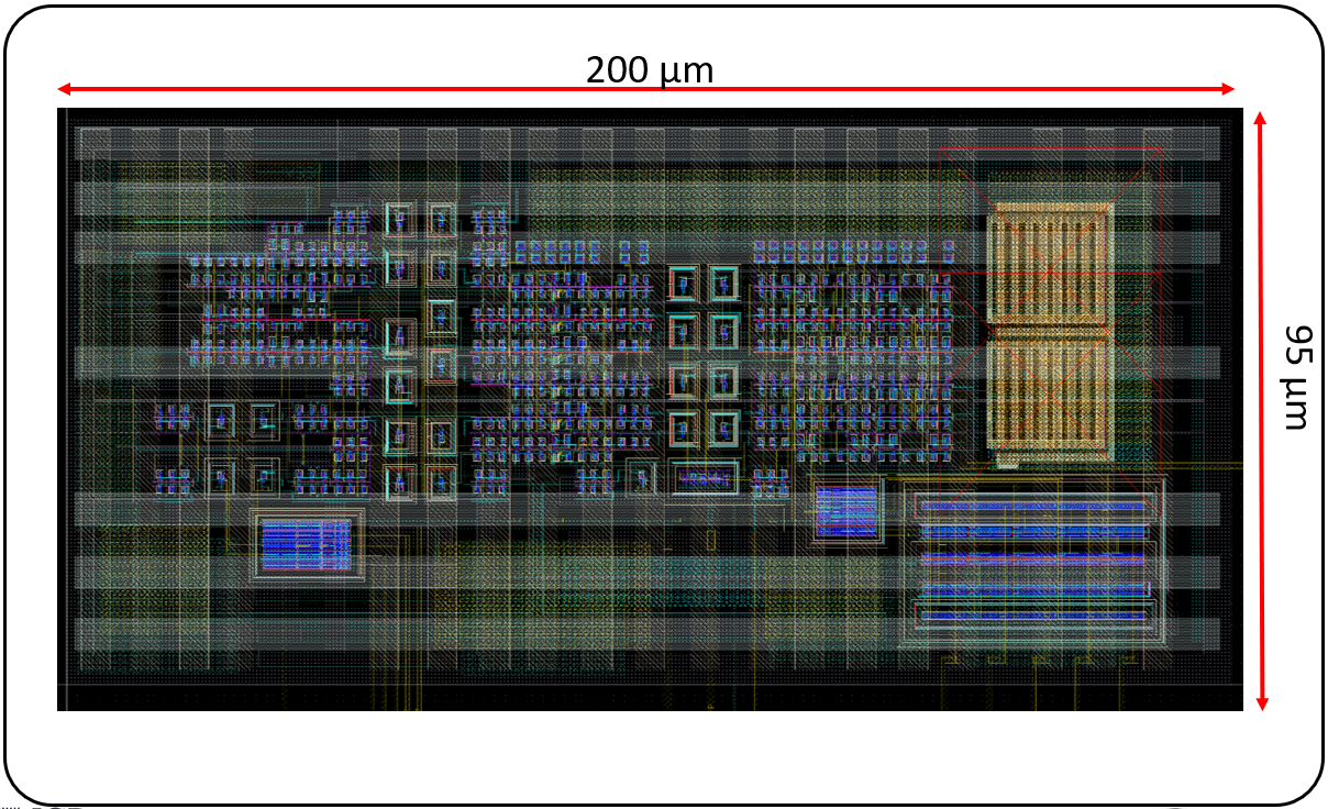
AC Logic Family
Block Diagram
Layout
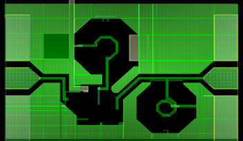
Spatial Sigma Delta ADC for MIMO
Block Diagram
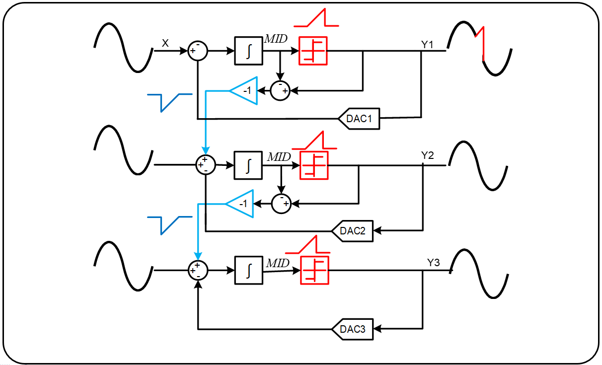
Layout
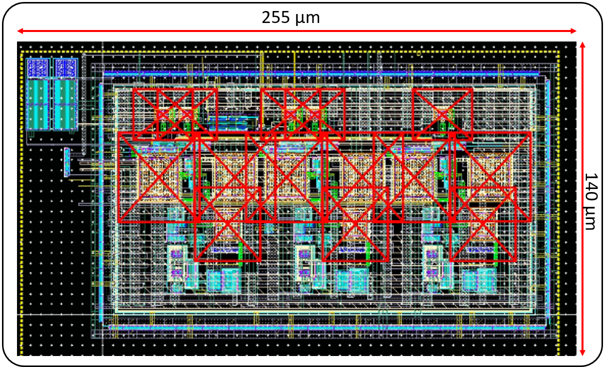
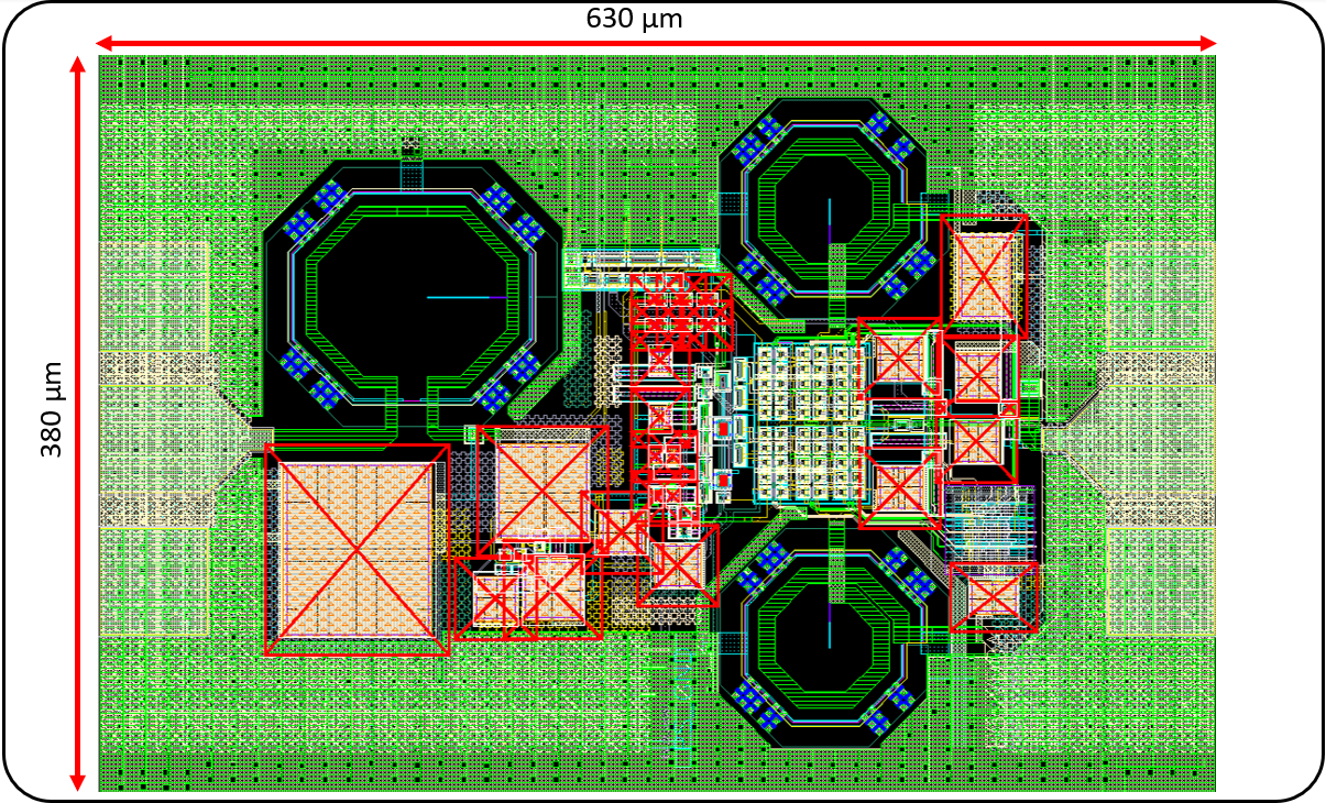
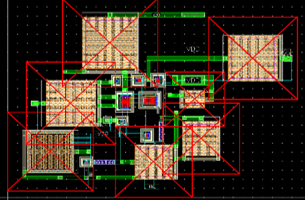
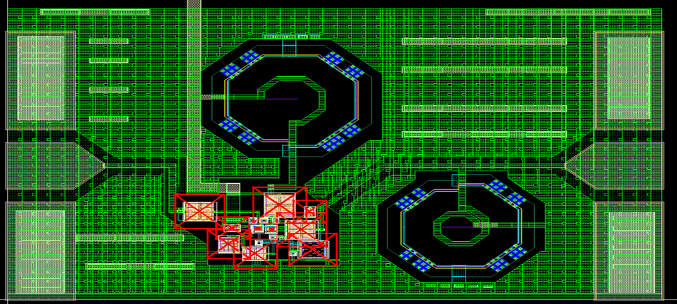
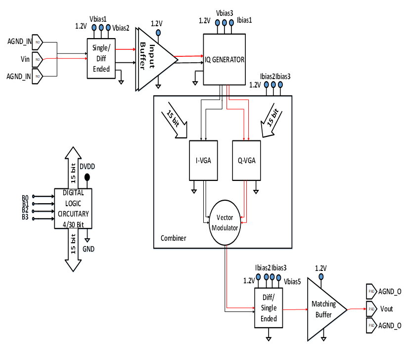
Mm-Wave Phase Shifters for MMIMO
Top Level Description
- Input and output probing through GSG probes
- Analog Voltage and digital Voltage supplies are provided for analog and digital circuitry, separately.
- Voltage biasing and current biasing are done for each block to mitigate the process variation.
Block Diagram
Layout